VLSI Digital Design Interview Questions:-
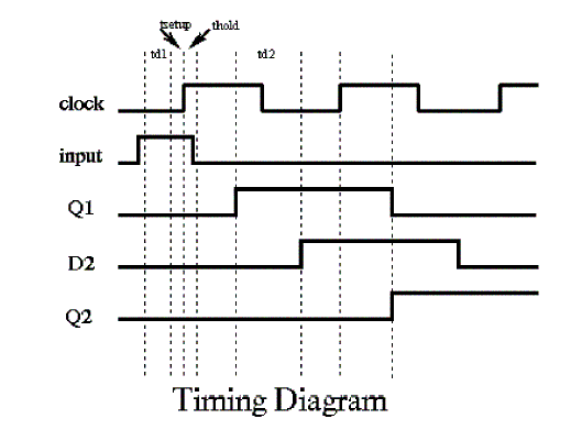
1) Explain about setup time and hold time, what will happen if there is setup time and hold time violation, how to overcome this?
Solution.
For Synchronous flip-flops, we have special requirements for the inputs with respect to clock signal input they are
Setup Time: Minimum time Period during which data must be stable before the clock makes a valid transition. E.g. for a positive edge triggered flip-flop having a setup time of 2ns so input data should be Stable for 2ns before the clock makes a valid transaction from zero to one.
Hold Time: Minimum time period during which data must be stable after the clock has made a valid transition. E.g. for a posedge triggered flip-flop, with a hold time of 1 ns. Input Data (i.e. R and S in the case of RS flip-flop) should be stable for at least 1 ns after clock has made transition from 0 to 1. Hold time is the amount of time after the clock edge that same input signal has to be held before changing it to make sure it is sensed properly at the clock edge.

Whenever there are setup and hold time violations in any flip-flop, it enters a state where its output is unpredictable: this state is known as metastable state (quasi stable state); at the end of metastable state, the flip-flop settles down to either '1' or '0'. This whole process is known as metastability.
2) What is difference between latch and flip-flop?
Solution.
The main difference between latch and FF is that latches are level sensitive while FF is edge sensitive. They both require the use of clock signal and are used in sequential logic. For a latch, the output tracks the input when the clock signal is high, so as long as the clock is logic 1, the output can change if the input also changes. FF on the other hand, will store the input only when there is a rising/falling edge of the clock. Latch is sensitive to glitches on enable pin, whereas flip-flop is immune to glitches. Latches take fewer gates (also less power) to implement than flip-flops. Latches are faster than flip-flops.
3) Given only two xor gates one must function as buffer and another as inverter?
Solution.
Tie one of xor gates input to 1 it will act as inverter.
Tie one of xor gates input to 0 it will act as buffer.
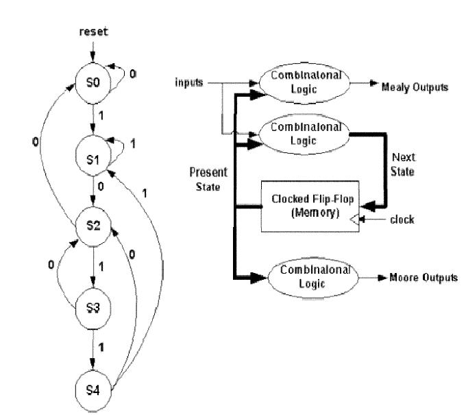
4) Difference between Mealy and Moore state machine?
Solution.
A) Mealy and Moore models are the basic models of state machines. A state machine which uses only Entry Actions, so that its output depends on the state, is called a Moore model. A state machine which uses only Input Actions, so that the output depends on the state and also on inputs, is called a Mealy model. The models selected will influence a design but there are no general indications as to which model is better. Choice of a model depends on the application, execution means (for instance, hardware systems are usually best realized as Moore models) and personal preferences of a designer or programmer
B) Mealy machine has outputs that depend on the state and input (thus, the FSM has the output written on edges). Moore machine has outputs that depend on state only (thus, the FSM has the output written in the state itself.
Advantage and Disadvantage
-> In Mealy as the output variable is a function both input and state, changes of state of the state variables will be delayed with respect to changes of signal level in the input variables, there are possibilities of glitches appearing in the output variables.
-> Moore overcomes glitches as output dependent on only states and not the input signal level.
-> All of the concepts can be applied to Moore-model state machines because any Moore state machine can be implemented as a Mealy state machine, although the converse is not true.
-> Moore machine: the outputs are properties of states themselves... which means that you get the output after the machine reaches a particular state, or to get some output your machine has to be taken to a state which provides you the output. The outputs are held until you go to some other state.
-> Mealy machine: Mealy machines give you outputs instantly, that is immediately upon receiving input, but the output is not held after that
clock cycle.
5) Difference between one hot and binary encoding?
Solution.
Common classifications used to describe the state encoding of an FSM are Binary (or highly encoded) and One hot. A binary-encoded FSM design only requires as many flip-flops as are needed to uniquely encode the number of states in the state machine. The actual number of flip-flops required is equal to the ceiling of the log-base-2 of the number of states
in the FSM. A one hot FSM design requires a flip-flop for each state in the design and only one flip-flop (the flip-flop representing the current or "hot" state) is set at a time in a one hot FSM design. For a state machine with 9- 16 states, a binary FSM only requires 4 flip-flops while a one hot FSM requires a flip-flop for each state in the design FPGA vendors frequently recommend using a one hot state encoding style because flip-flops are plentiful in an FPGA and the combinational logic required to implement a one hot FSM design is typically smaller than most binary encoding styles. Since FPGA performance is typically related to the combinational logic size of the FPGA design, one hot FSMs typically run faster than a binary encoded FSM with larger combinational logic blocks.
6) Tell some of applications of buffer?
Solution.
-> They are used to introduce small delays.
-> They are used to eliminate cross talk caused due to inter electrode capacitance due to close routing.
-> They are used to support high fan-out, e.g.: bufg
7) Give two ways of converting a two input NAND gate to an inverter?
Solution.
-> Short the 2 inputs of the nand gate and apply the single input to it.
-> Connect the output to one of the input and the other to the input signal.
8) Why is most interrupts active low?
Solution.
This answers why most signals are active low. if you consider the transistor level of a module, active low means the capacitor in the output terminal gets charged or
discharged based on low to high and high to low transition respectively. When it goes from high to low it depends on the pull down resistor that pulls it down and it is relatively easy for the output capacitance to discharge rather than charging. Hence people prefer using active low signals.
9) Design a four-input NAND gate using only two-input NAND gates.
Solution.
F = (ABCD)’ = A'+B'+C'+D'
F = (A'+B')+(C'+D')
Using De-Morgan's theorem, we get F = (AB)'+(CD)'
10) What will happen if contents of register are shifter left, right?
Solution.
It is well known that in left shift all bits will be shifted left and LSB will be appended with 0 and in right shift all bits will be shifted right and MSB will be appended with 0 this is a straightforward answer. What is expected is in a left shift value gets Multiplied by 2 e.g.: consider 0000_1110=14 a left shift will make it 0001_110=28, it the same fashion right shift will Divide the value by 2.
11) What is a multiplexer?
Solution.
It's a combinational circuit that selects binary information from one of many input lines and directs it to a single output line.
For 2^n no. of inputs, we need n no. of selection lines.
12) What are set up time & hold time constraints? What do they signify? Which one is critical for estimating maximum clock frequency of a circuit?
Solution.
Set up time is the amount of time the data should be stable before the application of the clock signal, where as the hold time is the amount of time the data should be stable after the application of the clock. Setup time signifies maximum delay constraints; hold time is for minimum delay constraints. Setup time is critical for establishing the maximum clock frequency.
13) Given two ASICs. one has setup violation and the other has hold violation. how can they be made to work together without modifying the design?
Solution.
Slow the clock down on the one with setup violations..
And add redundant logic in the path where you have hold violations.
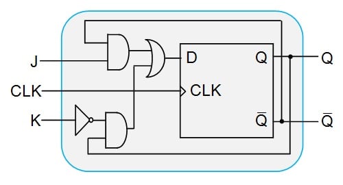
14) How can you convert an SR Flip-flop to a JK Flip-flop?
Solution.
By giving the feedback we can convert, i.e. !Q=>S and Q=>R.Hence the S and R inputs will act as J and K respectively.
15) How can you convert the JK Flip-flop to a D Flip-flop?
Solution.
By connecting the J input to the K through the inverter.

16) How can you convert the D Flip-flop to a JK Flip-flop ?
Solution.
To see general procedure for F.F. conversion:
https://www.allaboutcircuits.com/technical-articles/conversion-of-flip-flops/
17) How do you detect if two 8-bit signals are same?
Solution.
XOR each bits of A with B (for e.g. A [0] xor B [0]) and so on. The o/p of 8 xor gates is then given as i/p to an 8-i/p nor gate. if o/p is 1 then A=B.
18) Convert D-FF into divide by 2. (not latch) What is the max clock frequency the circuit can handle, given the following information ?
T_setup= 6ns
T_hold = 2nS
T_propagation = 10nS
Solution.
Circuit: Connect Qbar to D and apply the clk at clk of DFF and take the O/P at Q. It gives freq/2.
Max. Freq of operation= 1/(propagation delay+setup time) = 1/16ns = 62.5 MHz
19) 7 bit ring counter's initial state is 0100010. After how many clock cycles will it return to the initial state?
Solution.
6 cycles
20) Design all the gates (NOT, AND, OR, NAND, NOR, XOR, XNOR) using 2:1 Multiplexer?
Solution.
Using 2:1 Mux, (2 inputs, 1 output and a select line)
a) NOT :Give the input at the select line and connect I0 to 1 & I1 to 0. So if A is 1, we will get I1 that is 0 at the O/P.
b) AND: Give input A at the select line and 0 to I0 and B to I1. O/p is A & B
c) OR: Give input A at the select line and 1 to I1 and B to I0. O/p will be A | B
d) NAND: AND + NOT implementations together
e) NOR: OR + NOT implementations together
f) XOR: A at the select line B at I0 and ~B at I1. ~B can be obtained from (a)
g) XNOR: A at the select line B at I1 and ~B at I0
21) N number of XNOR gates is connected in series such that the N inputs (A0, A1, A2......) are given in the following way: A0 & A1 to first XNOR gate and A2 & O/P of First XNOR to second XNOR gate and so on..... Nth XNOR gates output is final output. How does this circuit work? Explain in detail?
Solution.
If N=Odd, the circuit acts as even parity detector, i.e. the output will 1 if there are even number of 1's in the N input...This could also be called as odd parity generator since with this additional 1 as output the total number of 1's will be ODD. If N=Even, just the opposite, it will be Odd parity detector or Even Parity Generator.
22) What is Race-around problem? How can you rectify it?
Solution.
The clock pulse that remains in the 1 state while both J and K are equal to 1 will cause the output to complement again and repeat complementing until the pulse goes back to 0, this is called the race around problem. To avoid this undesirable operation, the clock pulse must have a time duration that is shorter than the propagation delay time of the F-F, this is restrictive so the alternative is master-slave or edge-triggered construction.
23) How will you implement a Full subtractor from a Full adder?
Solution.
All the bits of subtrahend should be connected to the NOT gate. The input carry bit to the full adder should be made 1. Then the full adder works like a full subtract.
24) What is difference between setup and hold time ?
Solution.
The interviewer was looking for one specific reason, and its really a good answer too..The hint is hold time doesn't depend on clock, why is it so...?
Setup violations are related to two edges of clock, i mean you can vary the clock frequency to correct setup violation. But for hold time, you are only concerned with one edge and do not basically depend on clock frequency.
25) In a 3-bit Johnson's counter what are the unused states?
Solution.
(2^n - 2n) is the one used to find the unused states in Johnson counter. So for a 3-bit counter it is 8-6=2.Unused states=2. the two unused states are 010 and 101
26) You have two counters counting upto 16, built from negedge DFF , First circuit is synchronous and second is "ripple" (cascading), Which circuit has a less propagation delay? Why?
Solution.
The synchronous counter will have lesser delay as the input to each flop is readily available before the clock edge. Whereas the cascade counter will take long time as the output of one flop is used as clock to the other. So the delay will be propagating.
For E.g.: 16 state counter = 4 bit counter = 4 Flip flops Let 10ns be the delay of each flop The worst case delay of ripple counter = 10 * 4 = 40ns The delay of synchronous counter = 10ns only.(Delay of 1 flop)
27) Design a circuit for finding the 9's compliment of a BCD number using 4-bit binary adder and some external logic gates?
Solution.
9's compliment is nothing but subtracting the given no from 9.So using a 4 bit binary adder we can just subtract the given binary no from 1001(i.e. 9).Here we can use the 2's compliment method addition.
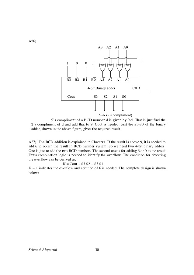
Eg:- To find the 9's compliment of 2 (0010)
-> 1's compliment of 0010 = 1101
-> Add 0001 to get the 2's compliment = 1110
-> Add this to 1001 (9) = (1) 0111
This can be tested in decimal: 0111 = 7, and 9 - 2 = 7.
Note that there was a carry bit (1) to the left. This indicates that the final answer is positive.
28) Implement the following circuits:
(a) 3 input NAND gate using min no of 2 input NAND Gates
(b) 3 input NOR gate using min no of 2 input NOR Gates
(c) 3 input XNOR gate using min no of 2 input XNOR Gates
Assuming 3 inputs A,B,C?
Solution.
3 input NAND Connect:
a) A and B to the first NAND gate
b) Output of first Nand gate is given to the two inputs of the second NAND gate (this basically realizes the inverter
functionality)4
c) Output of second NAND gate is given to the input of the third NAND gate, whose other input is C
((A NAND B) NAND (A NAND B)) NAND C Thus, can be implemented using '3' 2-input NAND gates. I guess this is the minimum number of gates that need to be used.
3 input NOR: Same as above just interchange NAND with NOR ((A NOR B) NOR (A NOR B)) NOR C.
3 input XNOR: Same as above except the inputs for the second XNOR gate, Output of the first XNOR gate is one of the
inputs and connect the second input to ground or logical '0'
((A XNOR B) XNOR 0)) XNOR C
29) What is glitch? What causes it (explain with waveform)? How to overcome it?
Solution.
The gated clock ‘s corresponding timing diagram shows that this implementation can lead to clock glitches ,Which can cause flip-flop to clock at the wrong time.
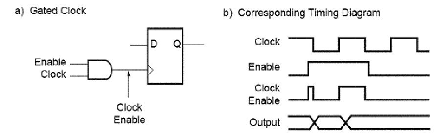
The following figure shows a synchronous alternative to the gated clock using a data path. The flip-flop is clocked at every clock cycle and the data path is controlled by an enable. When the enable is Low, the multiplexer feeds the output of the register back on itself. When the enable is High, new data is fed to the flip-flop and the register changes its state.

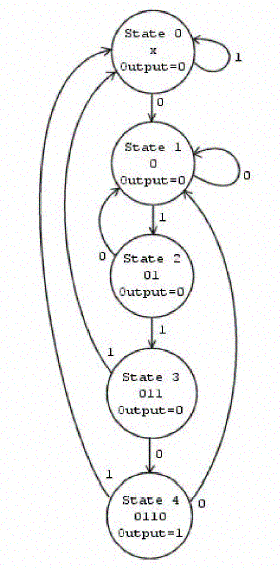
30) Draw the state diagram to output a "1" for one cycle if the sequence "0110" shows up (the leading 0s cannot be used in more than one sequence)?
Solution.
31) Design a FSM (Finite State Machine) to detect a sequence 10110?
Solution.
32) Give the circuit to extend the falling edge of the input by 2 clock pulses?
Solution.


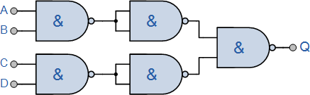
33) Draw timing diagrams for following circuit?
Solution.
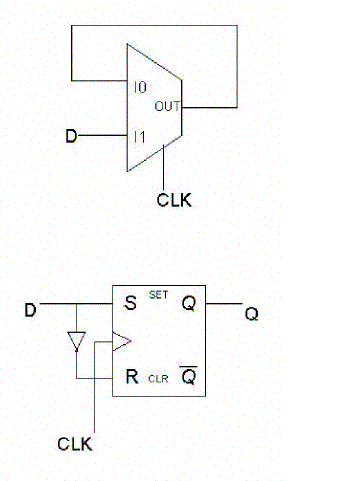
34) How to implement a Master Slave flip flop using a 2 to 1 Mux?
Solution.

35) Design a D-latch using (a) using 2:1 Mux (b) from S-R Latch?
Solution.
References :
1. Interview Questions => Must check-out CMOS Interview Question section from this.
2. Technical Bytes => Nice videos on STA, clock divider and general digital design concepts.
3. Digital Electronics Question Bank
4. http://www.asic-world.com/tidbits/index.html
5. Static Timing Analysis By VLSI Expert
Thank you for providing this knowledge I was searching for this information.
ReplyDeletePlease provide some more information regarding jobs.
Best job search website in Etobicoke Canada
This comment has been removed by the author.
ReplyDelete